


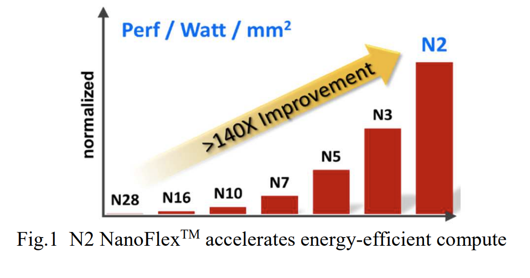
TSMC revealed additional details about its N2 (2nm class) manufacturing process at the IEEE International Electron Device Meeting (IEDM) earlier this month. The new production node promises 24-35% power savings or 15% performance improvement and 1.15x higher transistor density at the same voltage compared to the previous generation 3nm process. These benefits are in large part enabled by TSMC’s new gate-all-around (GAA) nanosheet transistors and the co-optimization capabilities of its N2 NanoFlex design technology and other enhancements detailed in the IEDM.
Gate-all-around nanosheet transistors allow designers to tune the channel width to balance performance and power efficiency. In addition, TSMC’s N2 adds the N2 NanoFlex DTCO, allowing designers to develop short cells with minimal area and increased power efficiency, or tall cells optimized for maximum performance. The technology also includes six voltage threshold levels (6-Vt) over a 200mV range and uses TSMC’s 3rd generation dipole-based integration with both n-type and p-type dipoles. It will be realized.
Image 1/3
N2 innovations introduced at the process and device level not only increase transistor drive current by improving sheet thickness, junctions, dopant activation, and stress engineering, but also increase effective capacitance (Ceff). The goal is also to achieve best-in-class energy efficiency. These improvements result in I/CV speed enhancements of approximately 70% and 110% for N-type and P-type nanosheet transistors, respectively.
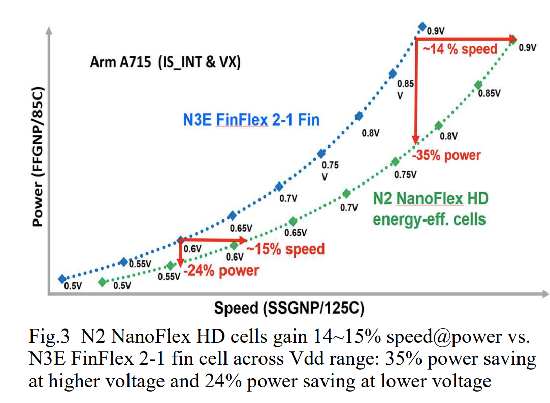
Compared to FinFETs, N2 nanosheet transistors offer significantly better performance per watt in the low supply voltage range of 0.5V to 0.6V. Process and device optimizations improve clocks by approximately 20% and reduce standby power consumption by approximately 75% at 0.5V operation. Additionally, the integration of N2 NanoFlex with multiple threshold voltage (multi-Vt) options provides even more flexibility in designing energy-efficient processors at high logic densities.
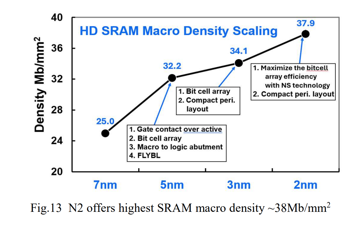
The advantages of transistor architecture and DTCO directly impact SRAM scalability, which has been difficult to achieve at recent state-of-the-art nodes. TSMC has successfully achieved a record 2nm SRAM density of approximately 38Mb/mm^2 using N2. In addition to achieving record SRAM density, TSMC also reduced power consumption. Since GAA nanosheet transistors feature a narrower threshold voltage variation (Vt-sigma), N2 provides approximately 20mV reduction in minimum operating voltage (Vmin) for high current (HC) macros compared to N2; High-density (HD) macros provide 30-35mV reduction. FinFET-based design. These improvements enable stable SRAM read and write functionality down to approximately 0.4V while maintaining robust yield and reliability.
In addition to new transistors, TSMC’s N2 features all-new middle-of-line (MoL), back-end-of-line (BEOL), and far-BEOL interconnects to reduce resistance by 20% and improve performance efficiency . N2’s MoL now uses barrier-free tungsten interconnects, which reduces vertical gate contact (VG) resistance by 55% and increases ring oscillator frequency by approximately 6.2%. Additionally, the first metal layer (M1) is now created in one EUV exposure pass followed by one etching step (1P1E), reducing complexity, mask count, and overall process Increase efficiency. According to TSMC, using EUV 1P1E in M1 reduces the capacitance of standard cells by nearly 10%, saving multiple EUV masks. In addition, N2 reduces metal (My) and via (Vy) resistance by 10%.
Additionally, additional features of the N2 for HPC applications include ultra-high performance MiM (SHP-MiM) capacitors that provide approximately 200fF/mm² of capacitance, which reduces transient voltage droop. A higher maximum operating frequency (Fmax) can be achieved.
Finally, TSMC’s N2 technology features a new Cu RDL option with TSV optimized for face-to-face and face-to-face 3D stacking with flat passivation and 4.5μm SoIC bond pitch, which will be an available feature. According to TSMC, it will also support AI, HPC, and even mobile design.
TSMC plans to begin production of its N2 process technology in the second half of 2025.