Amid growing demand for advanced packaging used in AI chips, TSMC Chairman CC Wei said during an earnings call in July that the company is working on a mini production line for FOPLP (fan-out panel level packaging). He acknowledged that results can be expected within three years. .
Here’s the latest information: According to Taiwanese media outlet MoneyDJ, the Taiwanese foundry giant has reportedly set initial specifications for FOPLP board size as it prefers a 300x300mm size rather than the rumored 515x510mm.
According to a report by MoneyDJ, equipment suppliers are working closely on the development of this technology, with mini-lines expected to be installed by as early as 2026 and gradually ramped up in 2027.
According to industry sources cited by MoneyDJ, TSMC initially preferred a rectangular board size of 515mmx510mm. However, due to “cost of ownership” (COO) factors and the maximum reticle size that could be supported, we ultimately chose to go with 300mx300mm.
The MoneyDJ report notes that TSMC is said to start with a size of 300x300mm, as larger substrate sizes not only exacerbate the warpage problem but also increase the risk of damage during transportation and packaging process transitions. , adding that they may consider expanding PLP packaging as substrate sizes change depending on future technology advances.
TSMC introduced FOWLP (Fan-Out Wafer Level Packaging) technology called InFO (Integrated Fan-Out) in 2016 and was first used in the iPhone 7’s A10 processor. Subsequently, demand for FOPLP solutions has increased as customers are attracted to more cost-effective solutions. Growing global demand for AI chips continues to put pressure on advanced packaging capabilities, increasing the need for FOPLP.
In addition to TSMC, Intel and Samsung are also making strides in this area. Samsung currently offers advanced packaging services such as I-Cube 2.5D packaging, X-Cube 3D IC packaging, and 2D FOPKG packaging. For applications that require low-power memory integration, such as mobile phones and wearable devices, Samsung already offers platforms such as fan-out panel-level packaging and fan-out wafer-level packaging.
Meanwhile, Intel plans to launch the industry’s first glass substrate solution for next-generation advanced packaging, with mass production expected between 2026 and 2030.
read more
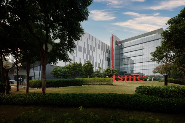
(Photo provided by: TSMC)
This article quotes the following information: money dj.
Previous article
(News) Rumor has it that SK Hynix will deliver a large HBM order to Broadcom in 2025
Next article
(News) Kioxia urges Bain and Toshiba to sell their shares, aiming to double AI NAND market share in three years


