


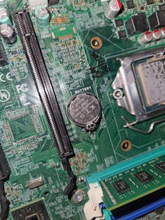
Our world’s rapid technological progress has been made possible by the ability to design and manufacture ever smaller electronic chips. They power computers, mobile phones, and every smart device ever introduced.
One of the many challenges is that as electronic components become smaller, they generate more and more heat. The key challenge is to make the wires that connect the transistors on the chip thinner while minimizing the amount of heat dissipated.
Manoranjan Mishra/Alamy
These interconnects are typically made of copper, and as they begin to scale down to nanoscale thickness, their electrical resistance rapidly decreases because electrons traveling along the wire are more likely to strike the surface of the wire. will increase to This is known as scattering and means energy is released in the form of waste heat and more power is required to maintain the same level of performance.
The Stanford University group created a thin film of a material known as niobium phosphide (NbP) that is 5 nanometers (nm) thick (the typical thickness of interconnects in today’s chips is about 10nm to 30nm). This improvement is due to the fact that NbP is a material with unique quantum properties.
NbP is a type of material known as a topological material, which has unique electronic properties due to its atomic structure and was the subject of the 2016 Nobel Prize in Physics. Electrical conductivity along the surface is very high and does not change as the shape or size of the material changes (physicists call this a “topologically protected surface state”).
In other words, it is sturdy and will not break easily even if deformed. Even when the material is thinned, bent, or textured, the special electrical conductivity found on its surface remains.
This is important because being able to reduce the thickness of electrical interconnects while still allowing electricity to flow easily is key to balancing manufacturing cost and complexity with energy efficiency. This gives NbP a significant advantage over other materials.
disorder and order
What’s particularly interesting about the Stanford team’s discovery is that these quantum properties were observed in disordered films. This means that niobium phosphide is not produced in the most controlled manner that maximizes its conductive properties.
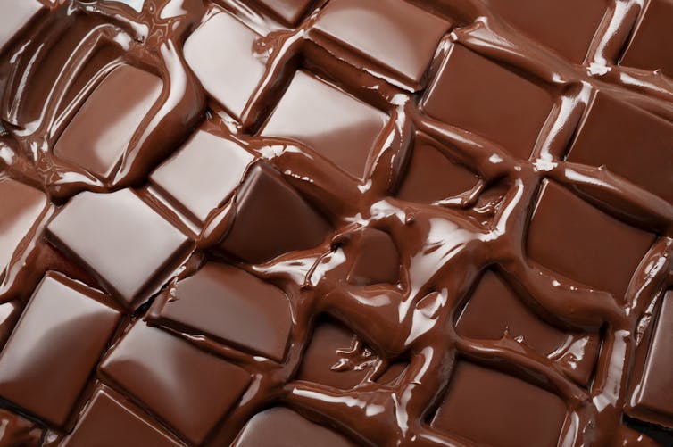
There is also a good analogy in the production of chocolate bars. Controlling the cooling process of melted chocolate is important to create a familiar, glossy final product. This process is known as tempering. Anyone who has tried this will know how dull and soft the untempered version is and how that affects the flavor.
The difference between tempered and untempered chocolate is the size (or, put another way, the amount of ordering) of the individual crystals within the chocolate’s structure. Untempered chocolate contains multiple small crystals that are disordered with each other. To make tempered chocolate, manufacturers cool the chocolate in a controlled manner and add tempered chocolate to promote the growth of a uniform crystal structure.
Elena..D
Imagine how convenient it would be if you could simply skip this tempering. This not only increases the efficiency of the production process, but also reduces the energy required. This is essentially what the Stanford team showed with their materials.
In technical terms, niobium phosphide had no long-range order. This means that the material was considered to be a disordered alloy overall, although it may have contained some small crystals reminiscent of the optimal version.
Nevertheless, it was still an excellent conductor for ultrathin films, likely due to the exotic quantum phenomenon of topologically protected surface states. If this effect can also occur in disordered materials, the manufacturing process will be significantly simplified, with a positive impact on costs.
This shows how quantum effects can lead to such significant improvements in electrical conductivity, potentially allowing us to produce more powerful and energy-efficient computer chips in the near future. One important question is whether sufficient quantities of niobium phosphide are available for manufacturing purposes.

Pulsar Images/Alamy
This is not our field, but phosphorus is about as abundant as carbon in the Earth’s crust, and niobium is about a third as abundant as copper and about as abundant as cobalt and nickel. This suggests that supplies are sufficient, but experts will need to weigh the relative costs of extracting these elements from ore.
For those of us working in this field, this finding also raises the question of whether other topological materials, such as tantalum phosphide and tantalum arsenide, may behave similarly. And what ingredients are required for NbP samples to behave this way? These questions will continue to engage scientists in the search for solutions that will enable future low-power computing technologies. Sho.