


Recently, global semiconductor giant Infineon Technologies has pioneered the development of the world’s first 300 mm power nitride (GAN) wafer technology. Gan Semiconductors have been used primarily in optically emitting diodes (LEDs) since the 1990s, but this advancement in this massive wafer technology is a major step forward in bringing both capabilities and cost-effectiveness to the industry.
The growing importance of GAN-based semiconductors is evident in sectors such as automobiles, computing and wireless communications, including 5G and radar systems. From AI system infrastructure and solar inverter power supplies to enabling EV chargers, adapters and motor control systems, GAN semiconductors are at the forefront of innovation requiring high-speed performance.
India’s semiconductor manufacturing capabilities lag behind its global peers, but the government’s ambition to position the country as a global semiconductor hub makes GAN technology a top priority for domestic research and development.
In 2022, the Nitrogen Ecosystem that enables Centres and Incubators (GEECI) to Enabling Gallium Nitride Ecosystems at the Indian Institute of Science (IISC) in Bengaluru, Minister of State for Skill Development and Entrepreneurship at the time. During his visit to (GEECI), Cancer emphasized that cancer can play a psychological role. In India’s quest to lead innovation in the automotive and mobility sector.
For decades, IISC and Bengaluru have been the center of semiconductor innovation and have nurtured many startups. One of these, Agnit SemiconductorsIndia’s first startup stands out as it focuses on developing Gan-based wafers.
Built from the ground up with proprietary technology and supported by over 15 years of research by top IISC professors and students, Agnit has enabled Gallium Ecosystem to enable the Gallium Ecosystem and incubator (GEECI) infrastructure, and is a Gan Wafer and Radio Frecurem (rf) ) Device production.
In the case of Agnit Scale, it is set to capture a growing market for gallium nitride semiconductor devices, which is expected to exceed $200 million by 2030. Deloitte Furthermore, it suggests that consumer electronics chargers are expected to make up 66% of the GAN chip market by 2026.
Agnit’s Deeptech Story
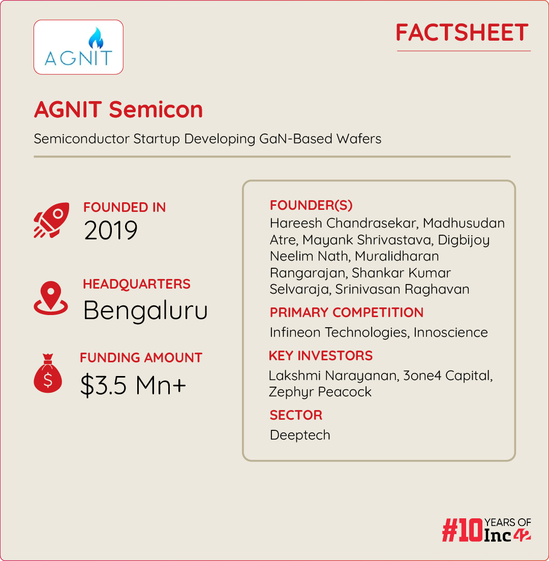
Agnit was founded in 2019 by seven industry experts (Hareesh Chandrasekar, Madhusudan Atre, Mayank Shrivastava, Digbijoy Nath, Muralidharan Rangarajan, Shankar Kumar Selvaraja and Srinivasan Raghavan).
Their expertise spans the entire GAN semiconductor ecosystem, from material growth and device manufacturing to integration of these devices into systems.
For context, Gan materials are deposited or grown on another silicon or silicon carbide in a process called epitaxy to develop a wafer. However, there were several prerequisites on the path to building an agnit, primarily solving the requirements of the manufacturing plant.
Speaking to MD and Inc42, co-founder of Raghavan’s Agnit, he said, “When there was a wave of fabs in India around 2015, I thought silicon was definitely something the country needs, but that’s what it was. I thought it was much more difficult. The fab required to bring out silicon chips is much larger… Gallium nitride per technology is not easy, but the fab required to start gallium nitride production in India The size is much easier.”
A team at IISC working on Gan Technology has once approached the government to set up Gan Foundry instead of a silicon foundry.
By then (around 2021), IISC Professor Ragavan and other co-founders had adopted Agnit and raised their first funding from Lakshminarayanan, former CEO of Cognizant Technologies, and had been carrying boats. Ta. Additionally, the Indian government’s financial support for IISC to build Geeci appeared after the two-year establishment of Agnit, helping semiconductors advance their efforts in the development of Gan Wafers.
span {Margin: 0;Padding: 3px 8px! important. font-size: 10px! Line-Height: 20px! important. Border Radius: 4px! important. font-weight: 400! falight;Font Style: Normal. Font family: noto sans, sans-serif;Color: #fff;Text spacing: 0! important. } .code-block.code-block-55 .tagged {margin: -4px 0 1px;padding: 0; Line-Height: Normal; } @media only screen and (max-width: 767px) {.code-block .code-block-55 {padding: 20px 10px; } .code-block.code-block-55 .recomended-Title {font-size: 16px; line height: 20px; margin bottom: 10px; } .code-block. code-block-55 .card-content {padding: 10px! fairity; } .code-block.code-block-55 {border-radius: 12px; padding bottom: 0; } .large-4.medium-4.small-6.column {padding: 3px; } .code-block .code-block-55 .card-wrapper.common-card diagram img {width: 100%; Min-Height: 120px! important. Max-Height: 120px! important. Object fit: Cover; } .code-block.code-block-55 .card-wrapper .taxonomy-wrap .post-category {padding: 0px 5px! Fality;Font size: 8px! Important; Height: Automatic! important. Line height: 15px; } .single .code-block.code-block-55 .entry-title.recommended-block-head a {font-size: 10px! comefict; Line-Height: 12px! important. } .code-block.code-block-55 .card-wrapper.common-card .meta-wrapper .meta .author a, .card-wrapper.common-card .meta-wrapper span {font-size:8px; } .code-block.code-block-55 .row.recomended-slider {overflow-x: auto;flex wrap: nowrap;padding bottom: 20px} .code-block.code-block-55 .type-post .card- wrapper .card-content .entry-title.recommended-block-head {line-height: 14px! Fality;Margin: 5px 0 10px! important. } .code-block.code-block-55 .card-wrapper.common-card .meta-wrapper span {font-size: 6px;margin: 0; } .code-block.code-block-55 .large-4 .medium-4.small-6.column {max-width: 48%; } .code-block.code-block-55 .sponsor-tag-v2> span {padding: 2px 5px! Fality;Font size: 8px! Important; font-weight: 400; Border radio: 4px; font-weight: 400; Font style: Normal. Font family: noto sans, sans-serif; Color: #fff; Character spacing: 0; Height: Automatic! important. } .code-block.code-block-55 .tagged {margin: 0 0 -4px;line height: 22px;padding: 0; } .code-block.code-block-55 a.sponsor-tag-v2 {margin :0; }})>
Currently, Agnit focuses primarily on the construction of Gan Wafers in silicon carbide, which is primarily compatible with RF applications, rather than the power electronics market. Its immediate potential markets will involve applications in strategic sectors such as defense radar, electronic warfare, and more.
Overall, the startup addresses the semiconductor and electronics manufacturing ecosystem in two ways. On the one hand, they develop and sell wafers to semiconductor fab companies, while on the other hand, they also sell separate RF power transistors built on top of GAN devices or wafers.
Agnit is buckling for device reliability checks and plans to create around one lark device in the next 12-24 months, so recently in a funding round co-led by 3One4 Capital and Zephyr Peacock We raised $3.5 million. From Narayanan at Cognizant.
Agnit Technology Focus and Challenges
Semiconductor manufacturing is capital-intensive and with Geeci’s support, Agnit can avoid building its own foundry. However, given Geeci has capabilities limitations, Agnit cannot build wafers that are larger than 8 inches. Therefore, you need to know how to build a 300 mm or 12 inch wafer that is suitable for the power electronics market.
Currently, along with the co-founder Digbijoy Nath, Agnit is leveraging technical know-how and existing features of GEECI to build 4-inch wafers in silicon carbide..
“Silicon Carbide can grow good quality gallium materials, but it’s a great platform with high prices. However, it is primarily for RF applications and the market is ready to pay this price. On silicon. Gallium nitride is relatively low cost and has much greater market opportunities, but Agnit also focuses on the former due to its strategic importance,” Nass added.
Meanwhile, Agnit aims to gradually expand into the power electronics market after establishing it in the main focus market.
Meanwhile, the founders said another challenge for them is to make wafer and RF devices global norms while keeping the startup focus intact.
In fact, Agnit aims to accommodate both global markets of Infineon, Mitsubishi Electric and Texas Instruments, as well as products facing competition from integrated device manufacturers such as Inloscience and Stanford Advanced Materials. .
However, most other startups working in GAN in India use global foundry to design subsystems or circuits, or purchase GAN modules from overseas, and domestic motorcycle modules or other They claimed to be creating power electronics.
The road beyond Agnit
Over the next 12 months, Agnit has turned to three key areas. Complete reliability qualifications, start production of components in the strategic market and enter the electronic electronic market.
Before Agnit can begin to produce a wealth of Gan RF devices, the company must qualify for reliability. It tests these devices under high temperatures, high power stress, and other conditions.
“Before commercial production begins, you must demonstrate that there is minimal decomposition or deterioration within acceptable limits according to industry standards. Reliability tests include various categories of car and space qualifications. Yes, but we’ll start with the basics,” says Nath.
This also hopes Agnit will record revenue in the next 12-24 months. Moreover, Raghavan highlighted the hunger for startups to add value to the broader domestic semiconductor ecosystem with manufacturing capabilities.
“We also aim to enable Indian semiconductor designers and Fabless startups that are currently dependent on companies outside of the country.
As the world moves towards high-computer devices and more efficient and smaller appliance devices, it will be interesting to track Agnit’s journey from here, especially when Gan as a technology is in its early stages.
(Edited by Shishir Parasher)